Shielding the Silicon: An Overview of Semiconductor Encapsulation Materials
Share
Semiconductor chips form the computing and intelligence backbone powering innovation across consumer electronics, automotive, aerospace, IoT systems, and industrial automation.
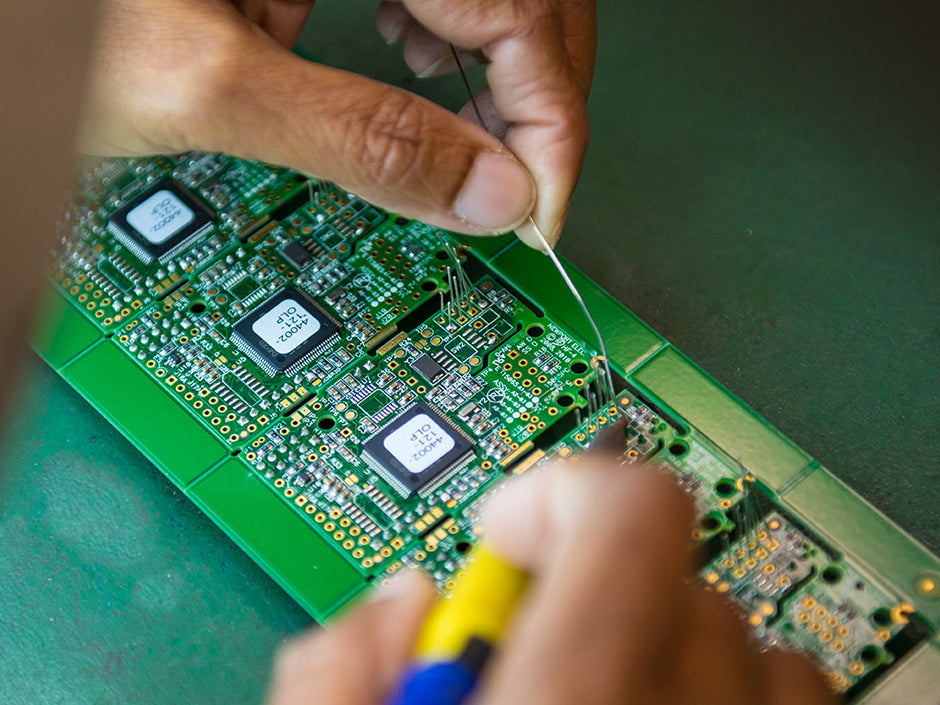
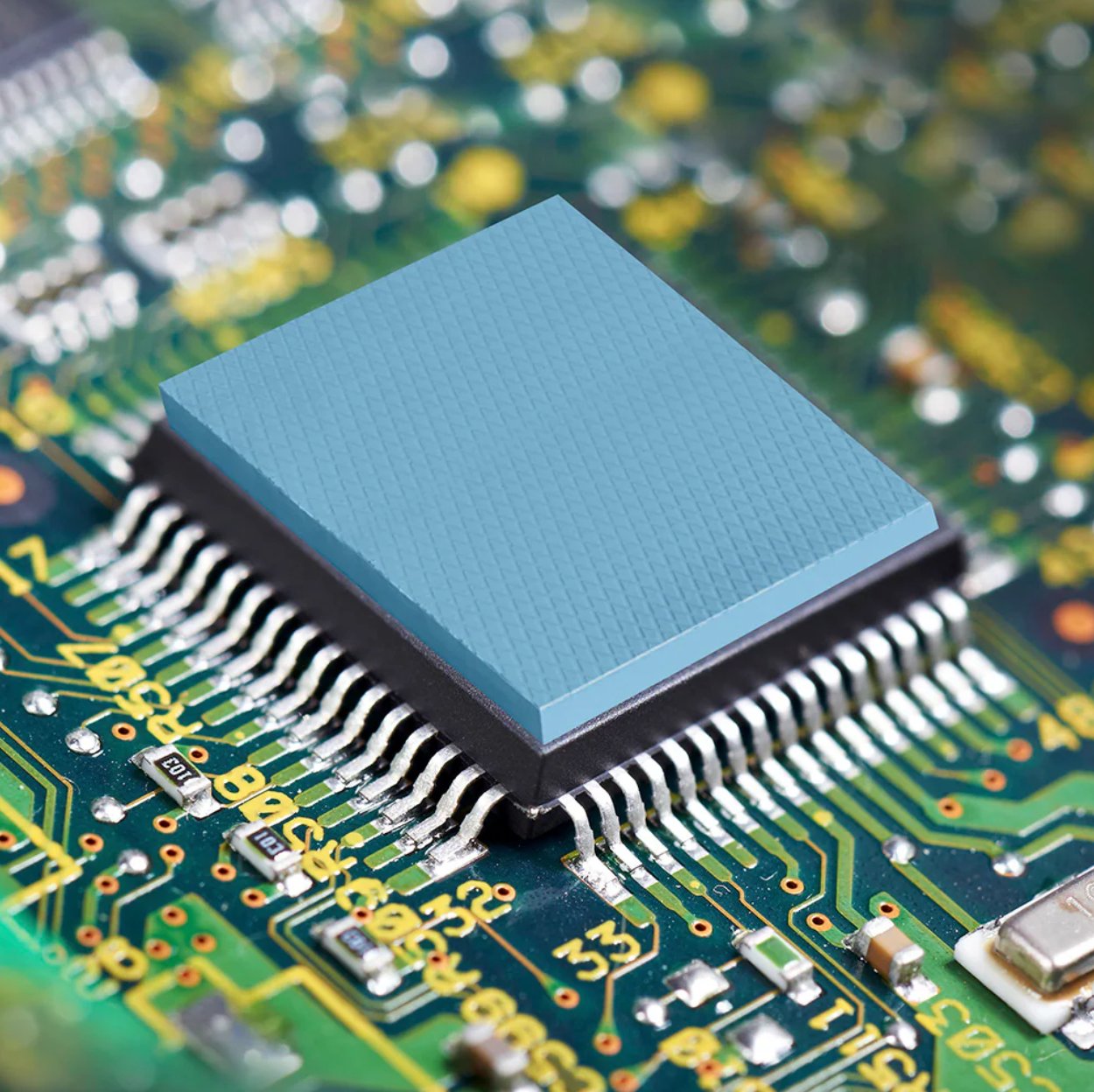
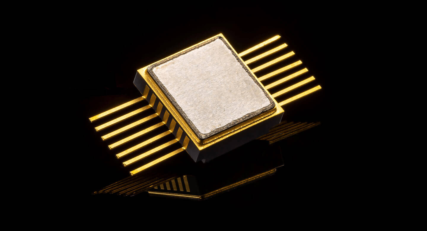
However, these fragile silicon dies with imprinted integrated circuits demand reliable protection from stresses, temperature fluctuations, humidity, chemicals, and other environmental threats over long operating lifetimes. This is achieved by semiconductor encapsulation using specialized materials as barriers against damage.
As a leader in advanced semiconductor packaging, American Fairfield offers an extensive portfolio of encapsulation materials and technology solutions to safeguard chip investments. This article provides an overview of key encapsulation materials and considerations for material and process selection.
Encapsulation Materials for Semiconductors
Polymeric encapsulants are applied over silicon dies on laminate substrates or lead frames through liquid dispensing, compression molding, or transfer molding techniques. Popular options include:
Epoxy Molding Compound
The workhorse for semiconductor encapsulation materials are epoxies that provide an optimal balance of protection, thermal conductivity, electrical resistance, and cost-effectiveness. Glob top and underfill epoxies also find extensive use.
Silicones
Softer encapsulants retain elastomeric properties across wide temperature swings (-55°C to 200°C) to absorb stresses from thermal cycling. Best for harsh environments.
Polyimides
Extremely heat-resistant encapsulants that withstand solder reflow temperatures beyond 300°C. Lower material costs than silicones.
Urethanes, UV-curable
Among other specialty encapsulant classes for niche requirements. It can be customized for specific CTE, hardness, and adhesion needs.
Technical Considerations for Encapsulant and Process Selection
With encapsulation playing a pivotal role in semiconductor reliability over 10-15nyear lifetimes, material properties and application parameters guide technology choices:
● Thermal Conductivity
Importance: Efficient heat dissipation is critical for preventing overheating of semiconductor devices, which can lead to performance degradation or outright failure. High thermal conductivity in the encapsulant helps to transfer heat away from hotspots on the chip, maintaining optimal operating temperatures.
Material Selection: Encapsulants with high thermal conductivity, such as certain epoxies or silicones filled with thermally conductive fillers like aluminum oxide or boron nitride, are preferred for applications where heat dissipation is a concern.
● Coefficient of Thermal Expansion (CTE) and Elastic Modulus:
Importance: CTE matching between the encapsulant, chip, and substrate is crucial to minimize thermal stress build-up, especially during temperature cycling or shock events. Mismatched CTEs can lead to mechanical failures such as delamination or cracking.
Material Selection: Encapsulants with CTE values closely matched to those of the semiconductor chip and substrate materials help reduce thermal stress.
Additionally, selecting encapsulants with appropriate elastic modulus ensures they can accommodate thermal expansion and contraction without causing mechanical strain on the encapsulated components.
● Temperature Cycling, Thermal Shock, and Wire Bond Reliability
Importance: Semiconductor devices often experience temperature variations during operation and thermal shock events during manufacturing or environmental exposure. The encapsulant should provide robust protection against thermal cycling-induced stresses and ensure the integrity of wire bonds.
Material Selection: Encapsulants with high thermal stability and mechanical strength, such as certain epoxies or polyurethanes, are chosen to withstand temperature cycling and thermal shock.
Additionally, considerations for wire bond reliability, such as adhesion to wire bond pads and minimal stress on bond wires, influence material selection.
● Dielectric Insulation
Importance: Encapsulants must provide high electrical insulation to prevent leakage currents and ensure the integrity of electronic circuits. Dielectric properties are particularly critical in high-voltage applications to avoid electrical breakdown.
Material Selection: Encapsulants with high dielectric strength and resistivity, such as certain silicones or epoxies, are preferred to maintain electrical insulation properties and prevent current leakage.
● Moisture Sensitivity
Importance: Moisture ingress can lead to corrosion of sensitive semiconductor components, affecting device reliability and performance. Encapsulants must resist moisture penetration and provide a protective barrier against humidity.
Material Selection: Encapsulants with low moisture absorption and excellent moisture barrier properties, such as certain silicone or epoxy formulations, are chosen to mitigate moisture sensitivity issues and ensure long-term reliability.
● Throughput, Yield, and Cost
Importance: Encapsulation processes should be scalable, efficient, and cost-effective to ensure high throughput and yield in semiconductor manufacturing. Material costs and processing considerations impact the overall economics of encapsulation.
Process Selection: Choosing encapsulation techniques that offer high throughput, such as molding or dispensing, can enhance manufacturing efficiency. Additionally, balancing material performance requirements with cost considerations is essential to optimize production costs.
Leveraging decades of expertise, American Fairfield’s technical teams address encapsulation challenges through cutting-edge materials and process insights to meet protection, reliability, and manufacturing goals.
Contact us to use semiconductor encapsulation capabilities honed over years of industry advances!